
Samsung Electronics Co., Ltd., a world-leading producer of high-performance memory devices, is announcing that it has begun mass production of the industry’s first 4-gigabyte (GB) DRAM package that is based on the 2nd generation High Bandwidth Memory (HBM2) interface. Targeted usage scenarios are high-performance computing, advanced graphics systems, advanced network systems, as well as enterprise servers. Samsung’s latest HBM solution offers unprecedented DRAM performance, to the tune of 7X faster than the current limits of DRAM performance. This allows for the faster responsiveness needed for high-end computing tasks such as graphics rendering, machine learning and parallel computing. The latest 4GB HBM2 DRAM utilizes Samsung’s most efficient 20-nm process technology and advanced HBM chip design to provide superior performance, energy efficiency and reliability in a small-dimensioned package that makes it ideal for the next generation of graphics cards and HPC systems.
 According to Sewon Chun, senior vice president of Memory Marketing for Samsung Electronics, “By mass producing next-generation HBM2 DRAM, we can contribute much more to the rapid adoption of next-generation HPC systems by global IT companies. Also, in using our 3D memory technology here, we can more proactively cope with the multifaceted needs of global IT, while at the same time strengthening the foundation for future growth of the DRAM market.”
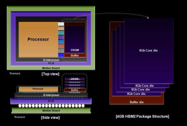
 Samsung’s new HBM2 DRAM marks the latest milestone in TSV (Through Silicon Via) DRAM technology, following on the heels of their 128GB 3D TSV DDR4 registered dual inline memory module (RDIMM) that was introduced in October of 2015. The 4GB HBM2 package is created by stacking four 8-gigabit (Gb) core dies on top of a buffer die at the bottom, which are then interconnected by TSV holes and microbumps. An individual 8Gb TSV HBM2 die contains over 5000 TSV holes, which is more than 36X that of a 8Gb TSV DDR4 die. This results in a significant improvement in data transmission performance as compared to a typical wire-bonding based package.
 Samsung’s newest DRAM package provides 2356GBps of bandwidth, which doubles that of HBM1 DRAM packages. The fastest data speed per pin among currently manufactured DRAM chips is the 36GBps of a 4Gb GDDR5 DRAM chip. The new HBM2 version offers a seven-fold increase over that level of performance. The 4GB HBM2 also provides enhanced power efficiency by effectively doubling the bandwidth per watt as compared to a 4Gb-GDDR5-based solution, as well as embedded ECC (error-correcting code) functionality, which results in high levels of reliability.
Samsung also plans to produce 8GB HBM2 DRAM packages later this year. When designers specify the 8GB HBM2 DRAM in graphics cards, they will be able to realize a space savings of more than 95% as compared to GDDR5 DRAM, which allows for the creation of more optimal solutions in compact devices that require high-level graphics computing capabilities. Samsung will steadily increase production of HBM2 DRAM over the balance of 2016 to meet anticipated market growth for servers and network systems. Samsung will also continue to expand its lineup of HBM2 DRAM offerings to continue to lead the way in the high-performance computing market and extend its lead in production of premium memory solutions.
![]() You can view the Samsung press release announcing the HMB2 DRAM in its entirety here.
You can view the Samsung press release announcing the HMB2 DRAM in its entirety here.